-
HOME
-
PRODUCTS
- High Speed Area Scan Camera
-
COAXPRESS SERIES-29MM CXP 1LANE SERIES
-
COAXPRESS SERIES-40MM CXP 1LANE SERIES
-
COAXPRESS SERIES-60MM CXP 4LANE SERIES
-
COAXPRESS SERIES-70MM CXP 4LANE SERIES
-
PIXEL SHIFT
-
SWIR Area Scan Camera
-
Camera Link Series
-
21MP CXP-12X4Lane Model
-
SOLUTIONS
-
SUPPORT
-
ABOUT US
-
CONTACT

- SOLUTION
 Semiconductor Solutions SOLUTIONS
- Summary
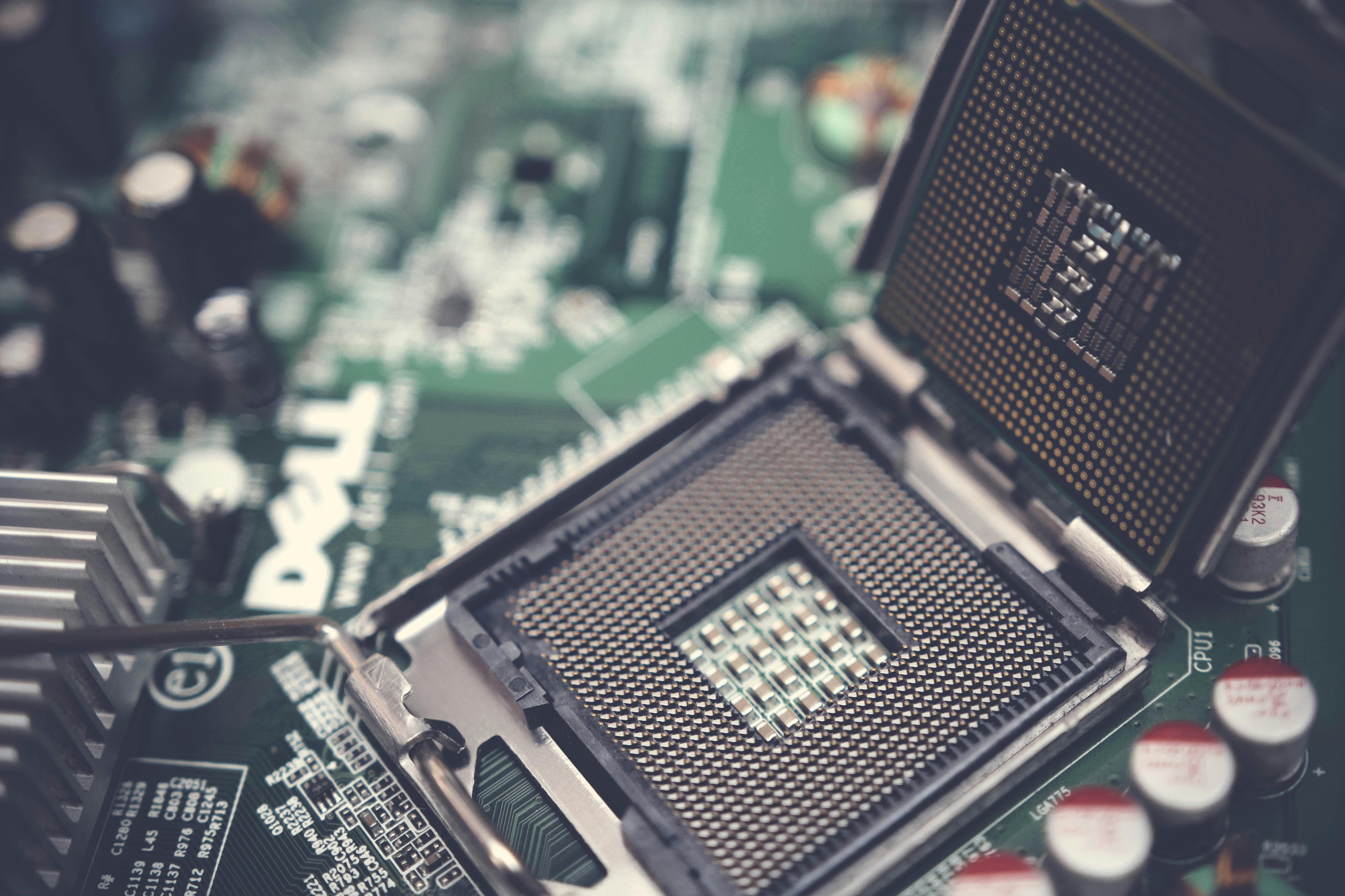
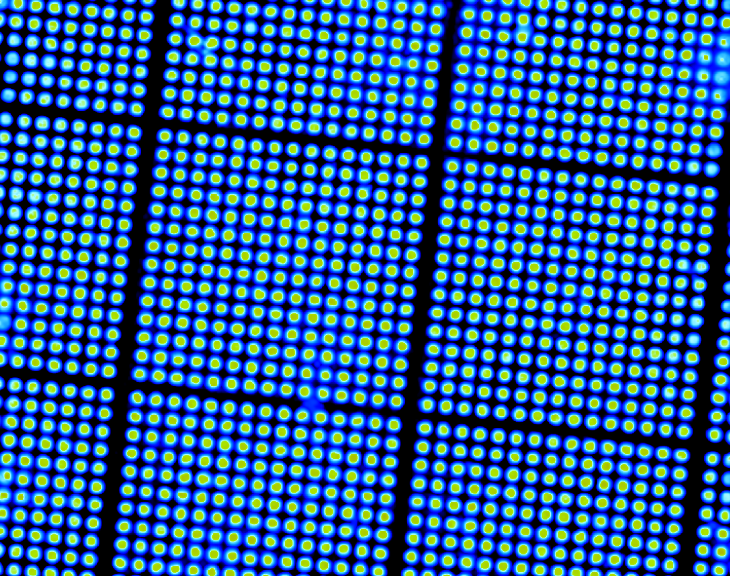
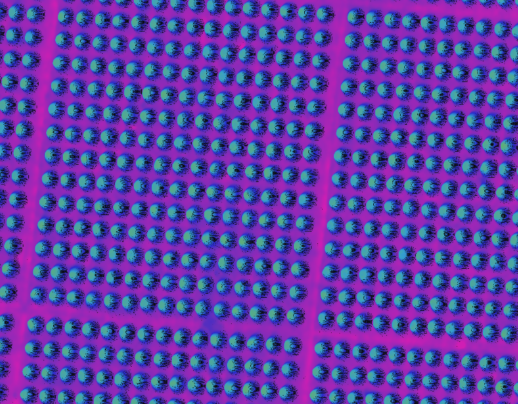
- Using Rindo MQP 3D camera system, 3D reconstruction of BGA chip can detect BGA tin ball height, volume, flatness and spacing data, and strictly control chip quality.
- Industry Overview
- At present, with the increasing demand for electronic products, the size of the semiconductor market continues to expand, and it also promotes the rapid development of the semiconductor testing market. At present, semiconductor testing is mainly used in electronic product manufacturing, automotive electronics, aerospace and other fields. At the same time, with the continuous progress of technology, new materials and new chips are also emerging, which also puts higher requirements on semiconductor detection technology.

 Solution Overview
For wafer/epitaxial wafer production and processing, semiconductor front/back surface defects, film thickness measurement, and various volume detection requirements in the Array segment of LCD/LED. Based on the self-developed ultra-high-speed, large-field, high-resolution imaging system combined with brain-inspired artificial intelligence technology, to create high-end detection equipment with completely independent intellectual property rights.
 Solution Difficulties
1
Difficult to image;
2
High precision;
3
High accuracy requirement;
4
Strong irregularity of defects;
 Solution Advantage
Large field of view
Wide imaging range, select the right lens can realize the full range of wafer detection
Low cost
Camera, light source, lens can be freely combined, effectively reduce the cost of equipment;
Fast speed
It takes a very short time to shoot an image with the area array image sensor.
Shooting Effect


- CONTACT INFORMATION
-
Address: 6 / F, Jingdong Technology Building, 76 Zhichun Road, Haidian District, Beijing
Telephone: 010-64754979
- Sales Consulting
-
E-Mail: sales@bopixel.com
Telephone: 139 1010 6272 Mr. Wang
- Technical Support
- E-Mail: support@bopixel.com
- PRODUCTS
- Structured Light 3D Camera
- High Speed Area Scan Camera
- HIGH SPEED LINE SCAN CAMERA
- DLP Projector
- Cr Series Code Reader & Industrial Smart Camera
- Ultra-high speed camera
- Line Laser 3D Profiler
- Frame Grabber
© 2023 Copyright Beijing BOPIXEL Technology Co., Ltd.Beijing Icp No. 2022013801


